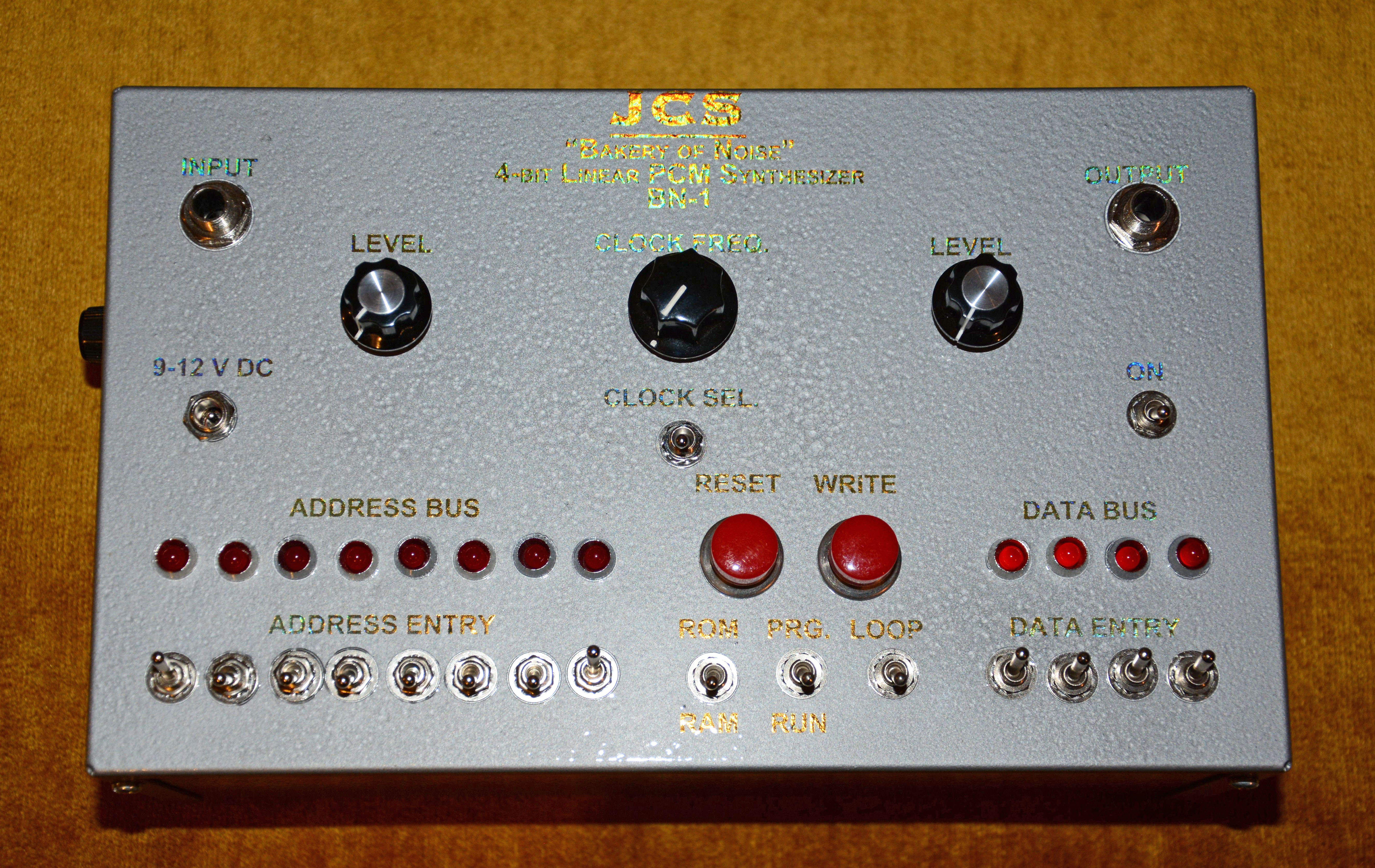
JCS "Bakery of Noise" BN-14-Bit Linear PCM Synthesizer
Before Crasno Electronics was created in mid-2017, I had a pseudo-company called JCS, short for "J-Corp Studios", that I created as a 10-year-old. Over the decade that it was used, the JCS name was applied to a website (now defunct), various CD albums, and the BN-1: the sole electronic device to bear it. When I decided to really go into business as a sole proprietorship, I discovered that the business name could not contain "corp" since it implies a corporation, and the acronym "JCS" had already been taken by many businesses across the world, and thus the name was abandoned. However, the overall styling and some of the collection articles of the Crasno website are only slightly modified from those of the old JCS site! In any case, enough history; on to the real subject of this article... Designed and built in mid-2015 (before I had taken any EE courses), the BN-1 is a rudimentary digital synthesizer using linear PCM sound generation, with 4-bit sample width and the unusual feature of allowing the sampling clock to be derived from an external frequency source such as an arbitrary musical instrument. It contains storage for 512 samples, half of which are stored in programmable SRAM, and the other half of which are stored in ROM. It was designed with versatility as well as serviceability in mind. All components are through-hole, and all ICs are socketed for easy replacement. The design most closely resembles IC-based digital circuitry of the 1970s. The circuitry of the BN-1 is mostly based on Soviet equivalents of standard TTL 74xx or 74LSxx series chips. In the schematics, the chips are denoted with both their 74xx / 74LSxx type, as well as another designation starting with "К155" (74xx) or "К555" (74LSxx), and denoting the equivalent type of chip made in the former Soviet Union. Few people know that you can purchase surplus Soviet-made parts of many kinds on eBay for quite cheap, and that they are of perfectly good quality—this is partially why I became interested in Russian and learned the alphabet. Anyway, one of the aims of this project was to make partial use of a large batch of Soviet ICs that I'd bought cheap on eBay, most being clones of Western logic chip types. There is only one Soviet chip used that there is no pin-compatible Western equivalent for, and that is the КР140УД1Б (transliterated: KR140UD1B), which is in fact a clone of the µA702 op-amp, the first type ever offered, but with a different pinout. Even so, all of the components are, as of late 2017, commonly available, and in many cases are able to be replaced with even more common equivalents with minor modification. The BN-1's sound depends significantly on the programmed series of samples being used and the clock source selected. However, no matter what, the sound tends to be "raw", "lo-fi", and "digital" sounding because the design incorporates no subtractive filtering and no amplitude control (besides the output level knob), and the 4-bit sample width makes for large steps between adjacent amplitude levels. In the future, a Crasno product may be introduced based on this device, though it would have numerous modifications, at the very least to provide a more appealing sound and more efficient user interface. It would also require a completely new PCB design and some hardware simplifications, since the build is extremely labor-intensive as it stands. More sensitive comparator circuits and additional frequency doubler stages would also be beneficial. In any case, I present the original design here for what it's worth, e.g. as a starting point for hobbyists looking to experiment with hardware-based digital synthesis. Features
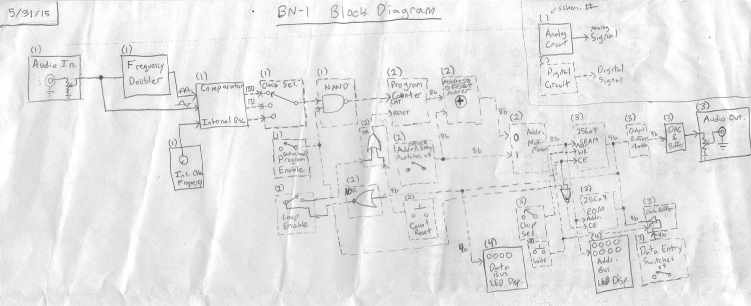
Design and ConstructionBlock Diagram and Schematic PreparationAs is often the case with electronic devices, this one started out with an overall idea: to design and build some type of linear PCM synthesizer. Then, some main specs were decided on, which were:
From these ideas, a block diagram was drawn on paper. As this block diagram progressed, so did a schematic that was started in the light edition of CadSoft EAGLE 7.2.0. Changes were made to the block diagram based on what was done in the schematic, as well as what was eventually done in the prototype. After many changes, a final block diagram was drawn on paper, and is shown below:
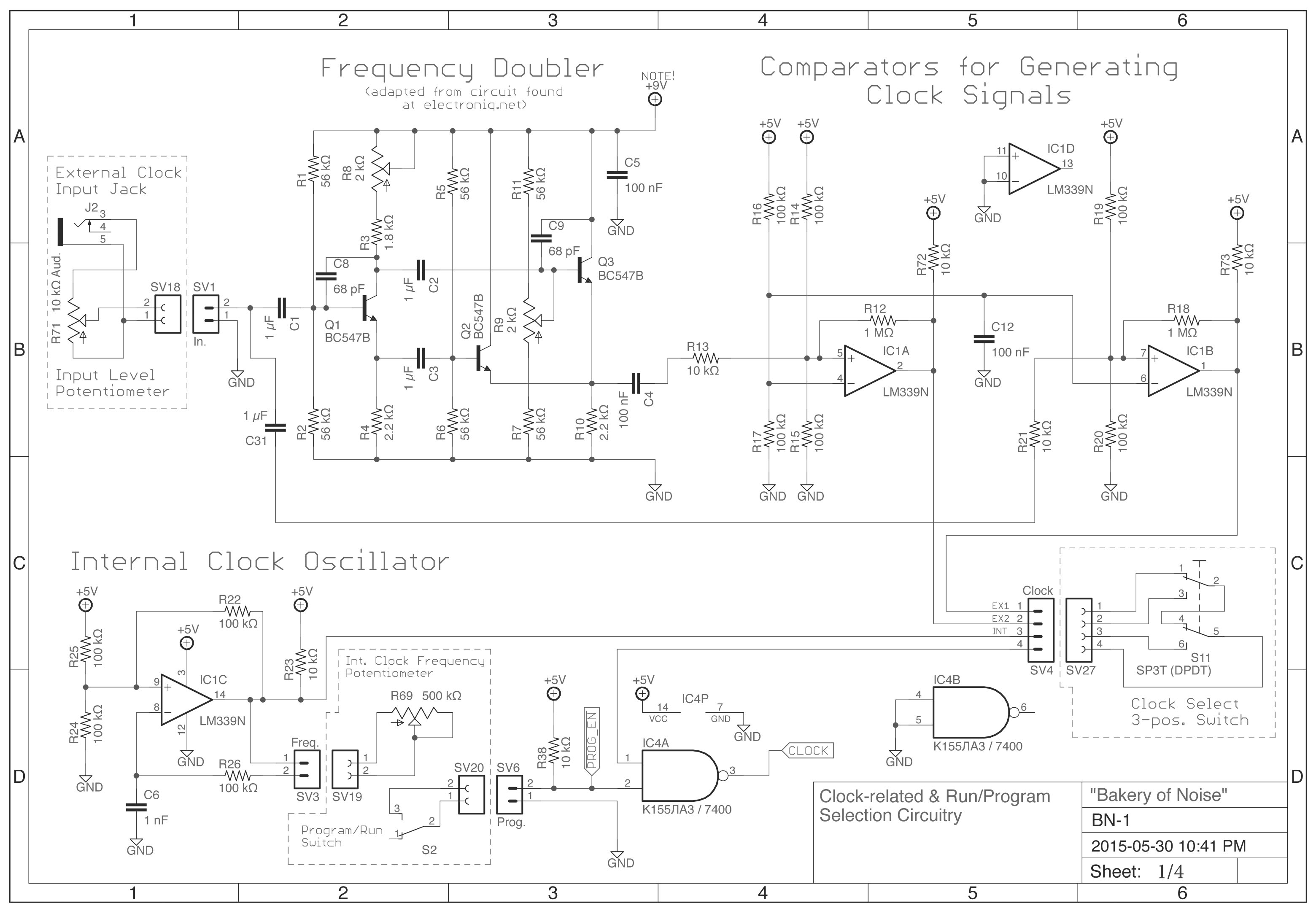
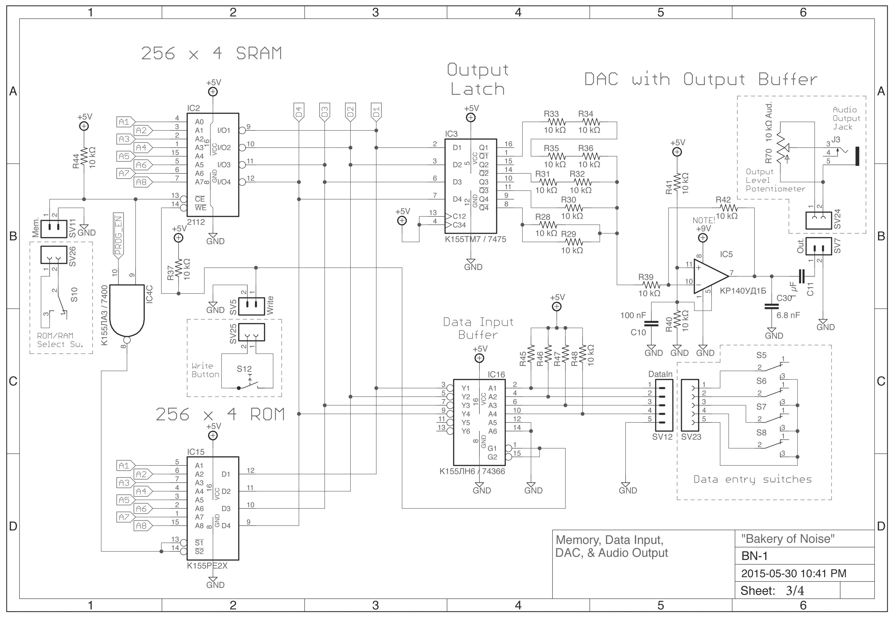
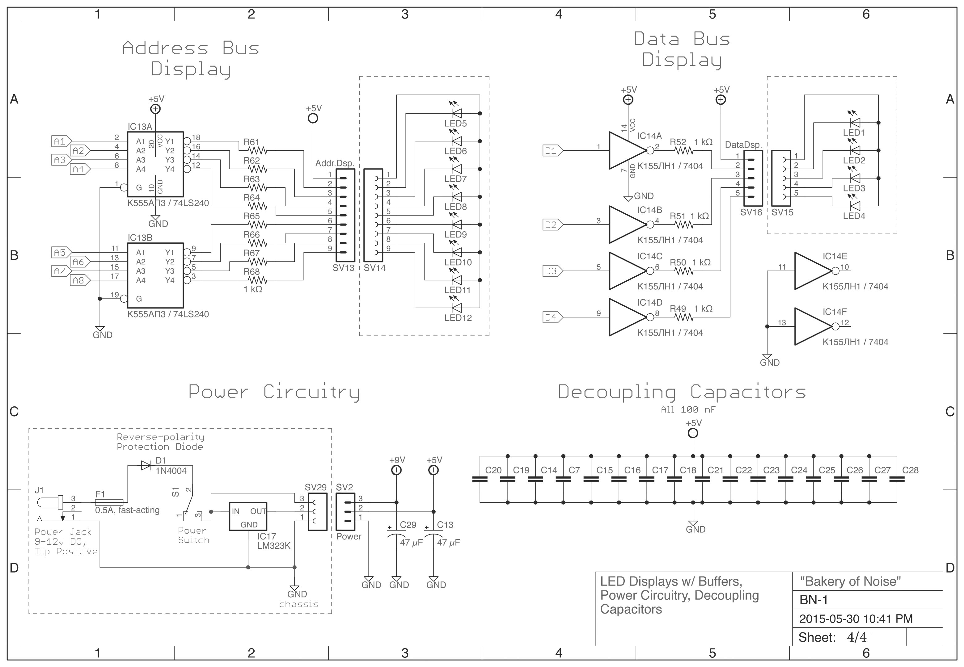
The schematic was prepared in four sheets using mostly standard parts from the EAGLE library. A few components had to be created, such as the 2112 SRAM and КР140УД1Б op-amp chips, which were not part of the default library. As well, the solder pad size of some of the default components was increased for ease of soldering as well as durability in the event something has to be desoldered. The finished sheets are shown below:
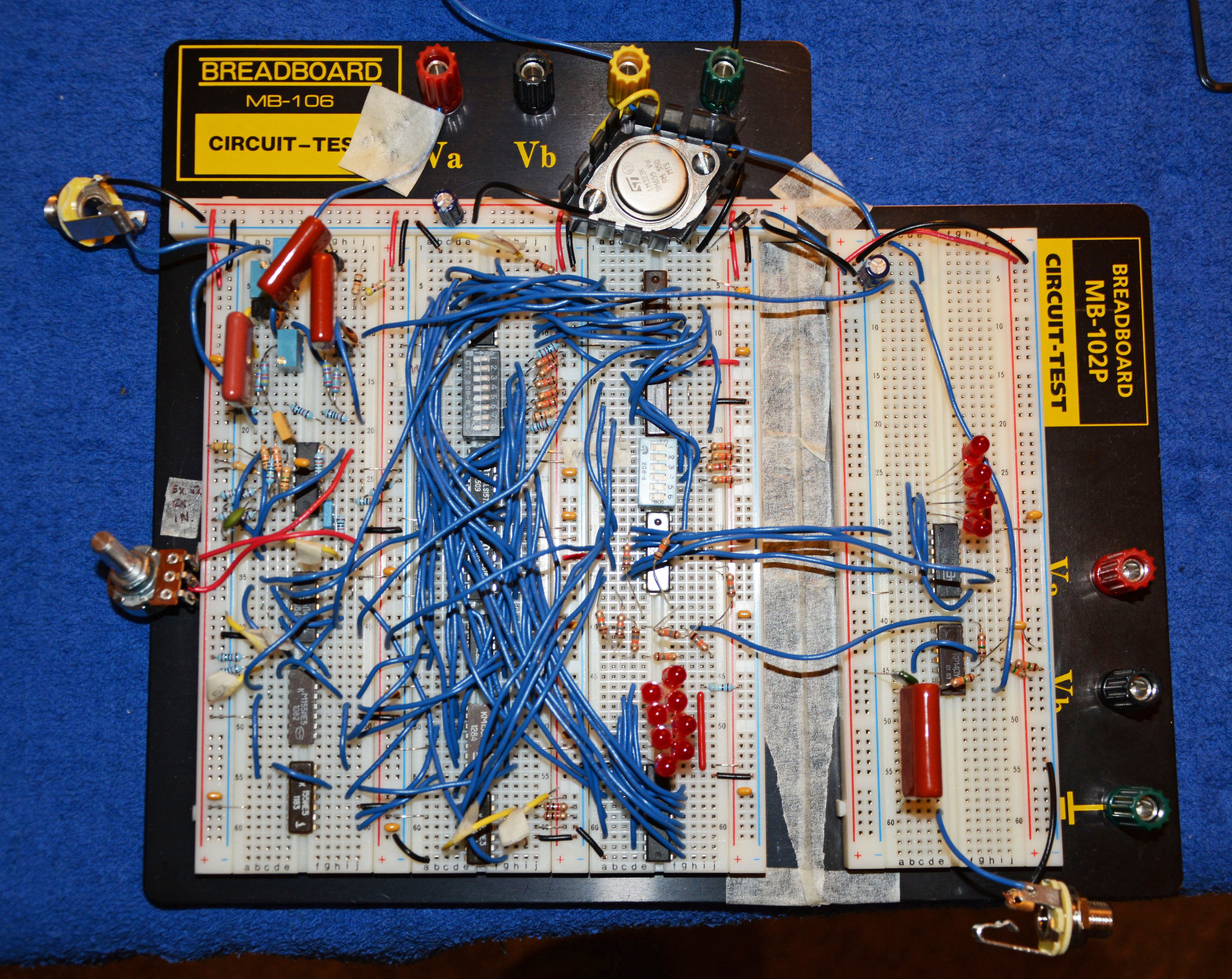
Alongside the preparation of the schematics, a prototype was assembled on breadboards. This allowed for testing the circuits as they were being designed, with revisions being made if the circuit did not work properly in practice. Certainly more fun than writing some code and programming a microcontroller! Here is the prototype, minus a few wires in the lower left, which were removed before the decision was made to photograph it.
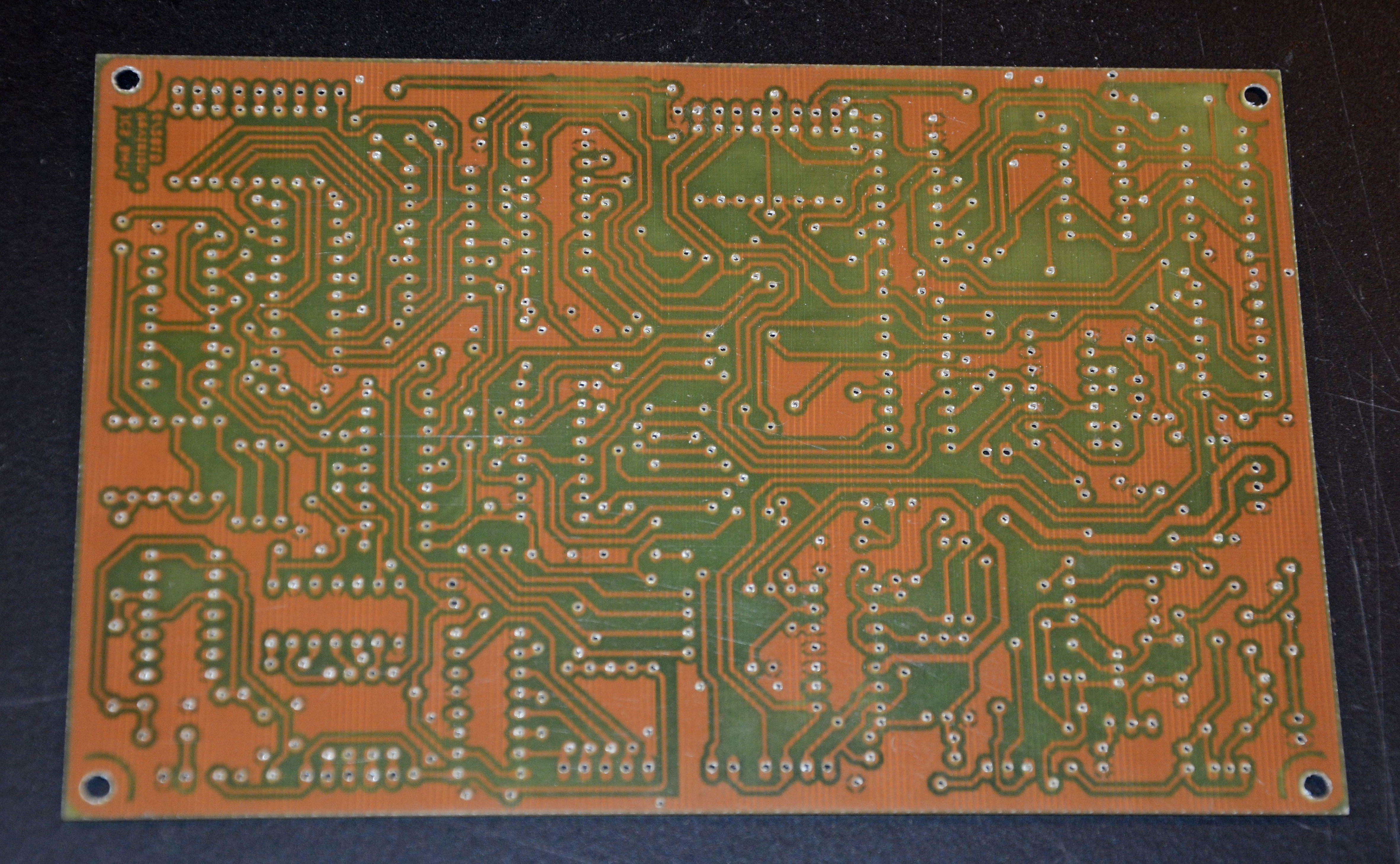
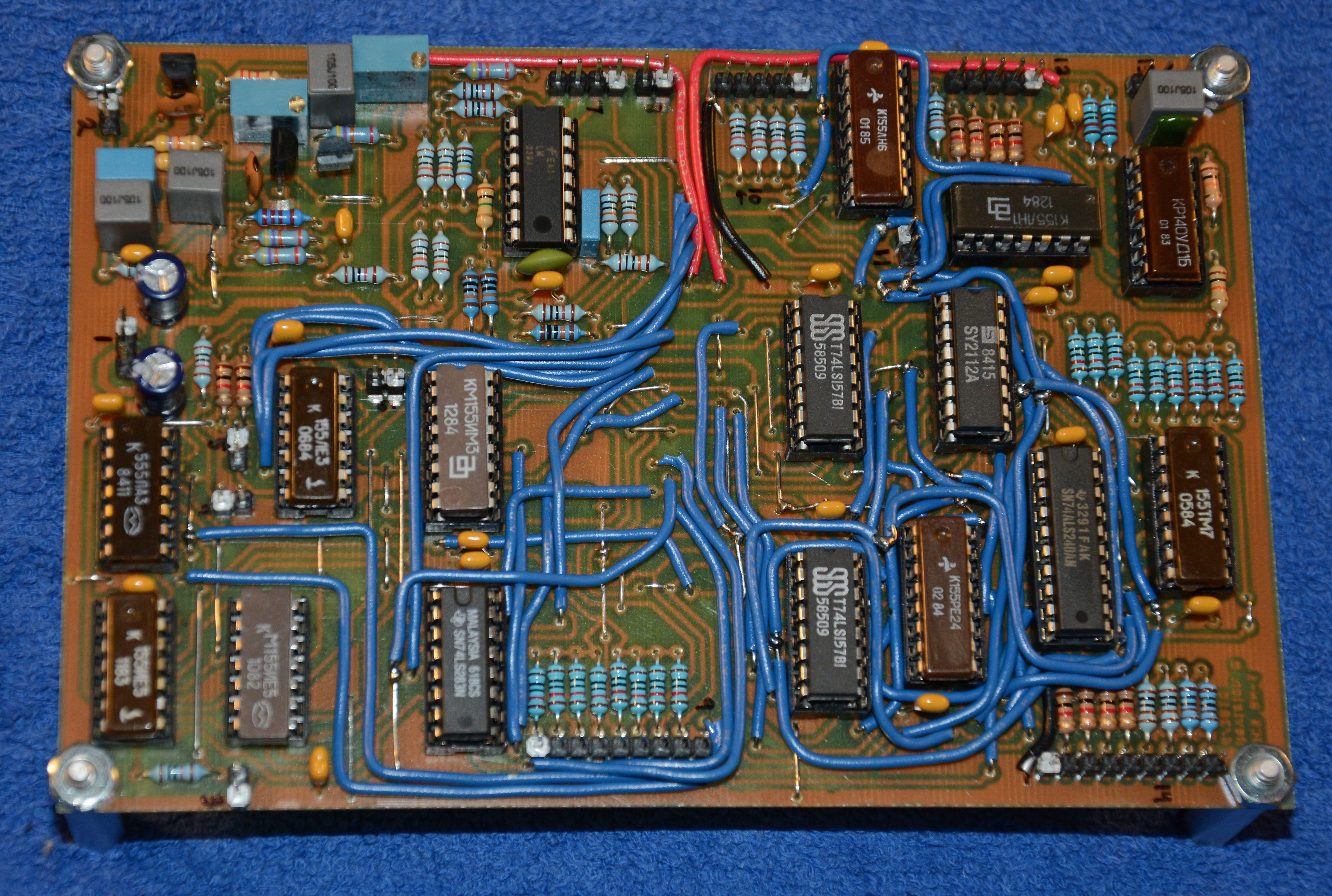
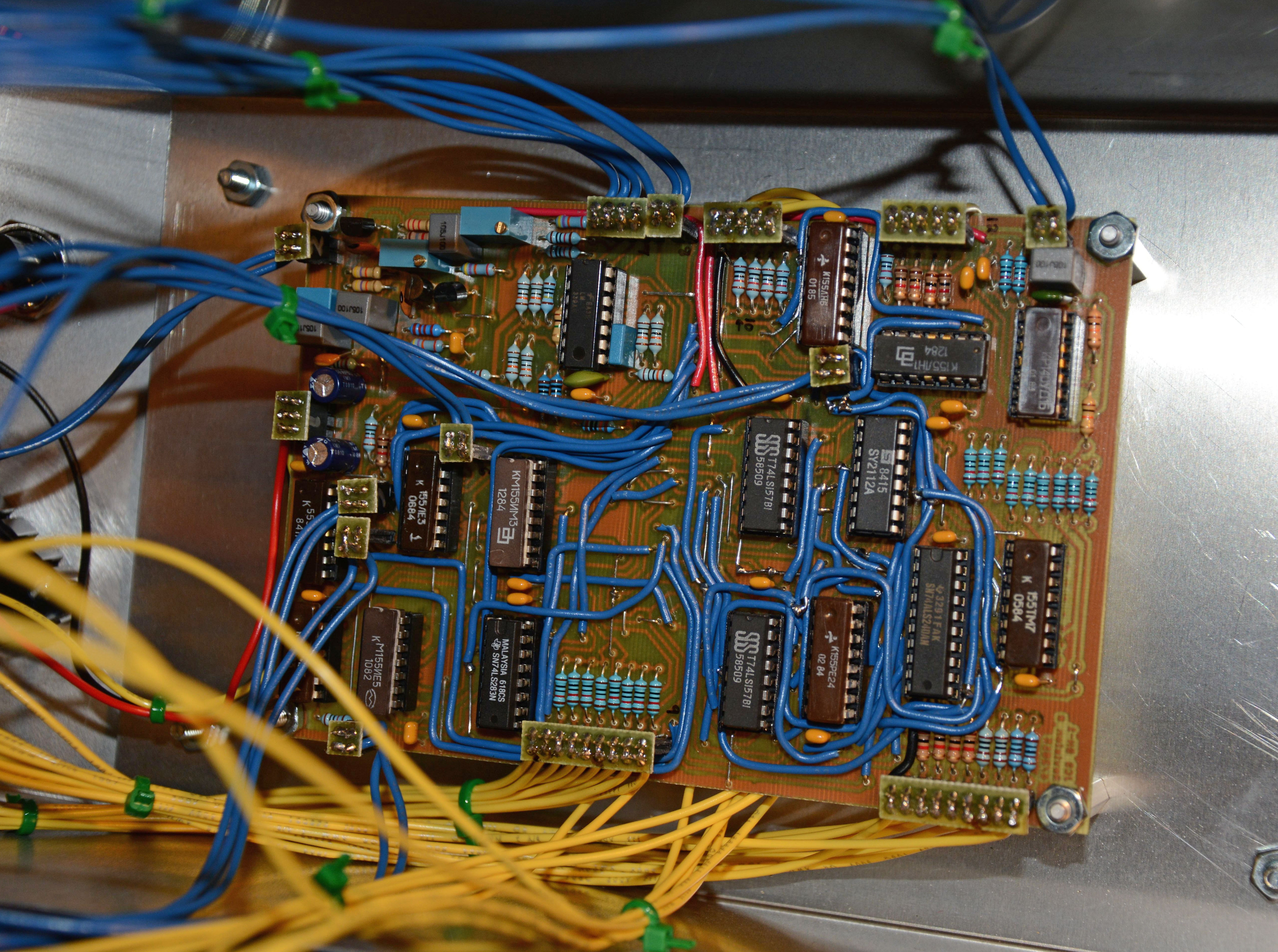
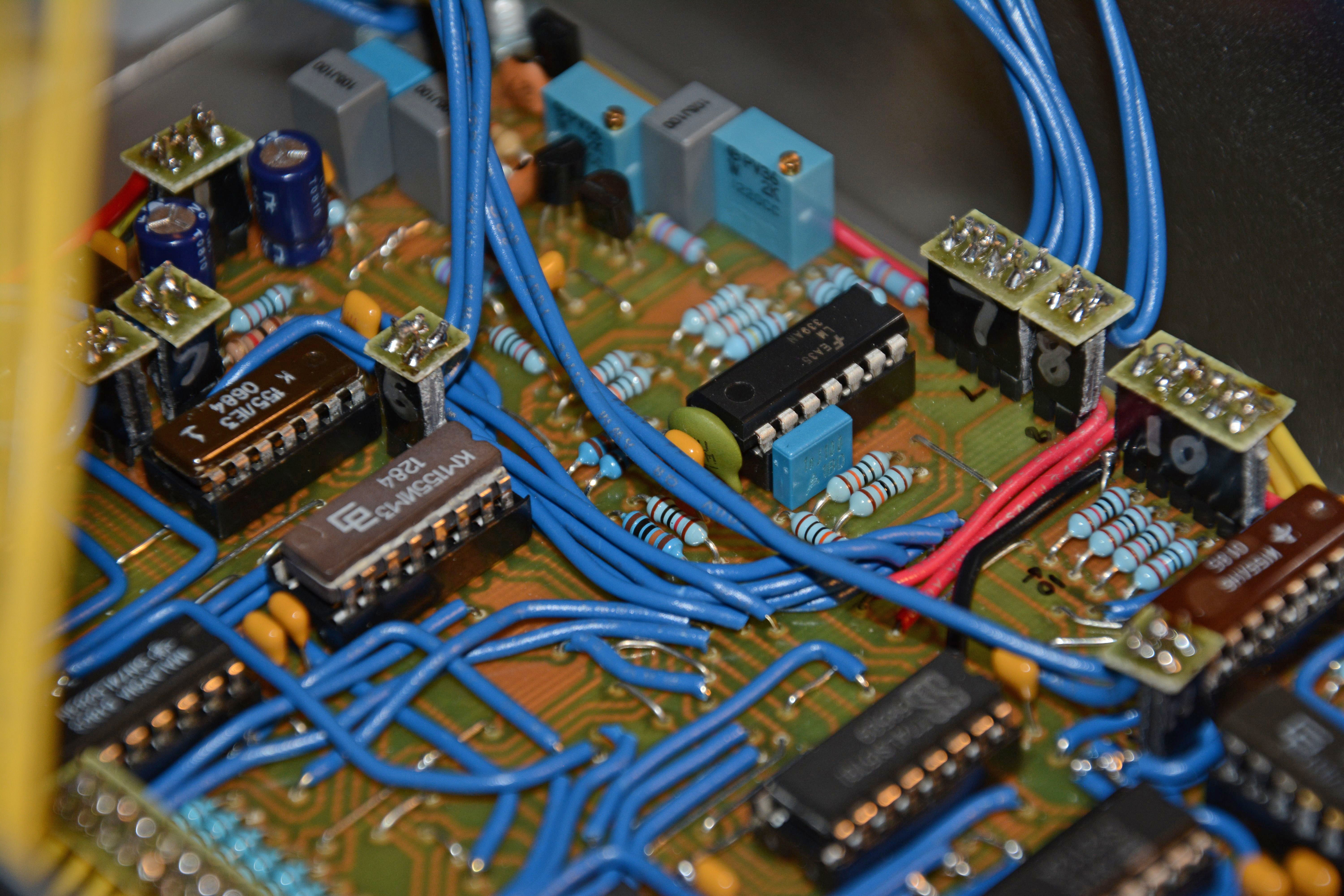
Note: I have decided to omit the detailed circuit description from this article. However, there is a zip file containing this detailed description, as well as some other useful information for those who are interested in understanding the circuit and possibly building it themselves. This can be found in the "Downloads" section at the bottom of the page. Design and Fabrication of the Printed Circuit BoardThe BN-1 has a single PCB that carries nearly all electronics besides controls and indicators. It is single-sided, measures almost exactly 4" x 6", and was designed in the light edition of EAGLE. Since the light edition restricts the maximum board size to 4" x 3.2", it had to be designed in two sections of about 4" x 3" each, which were later edited together in Photoshop. This resulted in considerable wasted space and an excessive number of jumper wires, particularly around the middle of the board, since the traces had to be arranged in such a way that they would line up on both sections. Another cause of wasted space was that I decided to use a relatively wide default trace width of 0.024" to reduce the chances of etching defects. Thus, the board design, while functional, is not ideal. Though, it was my second attempt at designing a PCB, and for that, I think its flaws can be partially excused. Nonetheless, I recommend to anyone interested in building this instrument to design their own PCB based on the schematics, instead of using my design. Once the board was designed, it was fabricated using the toner transfer method with Pulsar's "Toner Transfer Paper". The design was printed onto a sheet of this, cut out, and applied to a cleaned 4" x 6", 1-ounce, copper-clad fiberglass (FR4) board of thickness 1/32" using a small pouch laminator. Some "GreenTRF" foil was also applied as a coating on top of the toner using the laminator, in order to make the traces as difficult for the etchant to penetrate as possible. It was etched in ferric chloride, and with the copper traces tinned using MG Chemicals' "Liquid Tin," for greater solderability and resistance to oxidization. Quite a few holes had to be drilled as well (using a somewhat flimsy Dremel press), as can be seen on the finished, but unpopulated board:
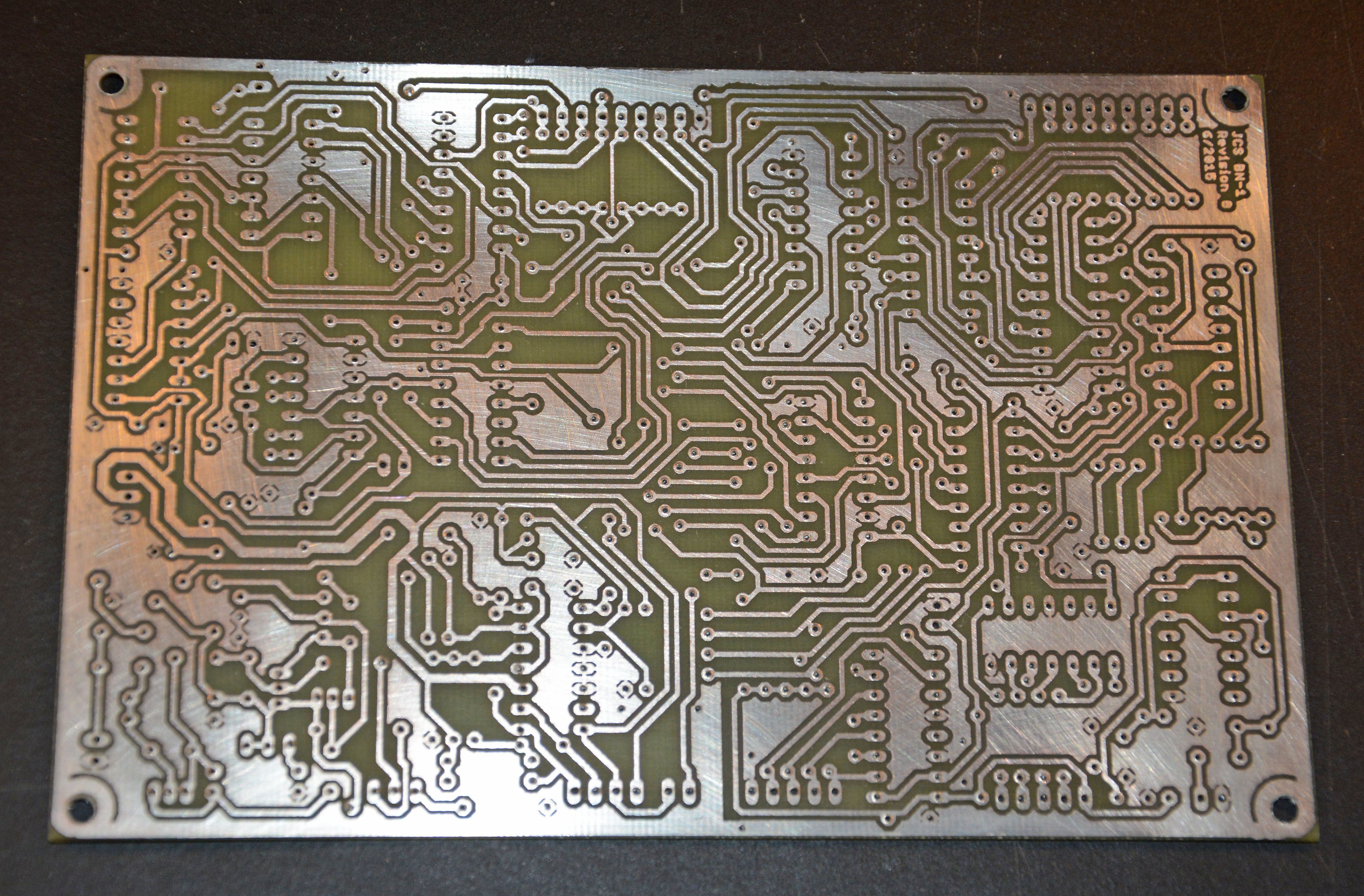
Components were mounted and soldered, with the finished board looking like this:
Enclosure & WiringFor the enclosure, a Hammond Manufacturing 1411UU utility case was used, with dimensions 10.0" x 6.0" x 3.5". A design for the component layouts on the top and side were produced in Photoshop, printed onto standard letter paper, and glued to the enclosure with Sulky KK2000 temporary spray adhesive. Then the component holes were drilled with a handheld drill, the visible surfaces sanded and cleaned, and about four coats of silver "hammered metal" paint applied after a single coat of grey primer (which may not have been necessary). The sanding included rounding the sharp edges of the enclosure for personal safety reasons. Lettering was applied to the top of the enclosure using Pulsar's "DecalPRO" system. Here are the general steps: First, the design, which is a binary image with large black borders around it, is printed as thickly as possible using a laser printer onto the "Toner Transfer Paper", which is then cut to size, and dried using a hot air gun. The direction that the paper curls when drying is memorized. Then, a sheet of "Toner Reactive Foil" is chosen that will give the black toner a coating of color. (In this case, I chose iridescent gold, which turned out to be a bit difficult to see against the silver hammered paint.) The paper is laid toner-side-up on a fiberglass board with the "TRF" laid face-down on it, and with a clear mylar sheet on top of all. It is fed through a small pouch laminator, which bonds the TRF to the toner. Once the TRF is removed, any excess left behind is taken off with blue painter's tape, and both the toner transfer paper and a sheet of mylar cut to be the same size as the paper are cleaned with isopropyl alcohol. Then, this is run through the laminator on the fiberglass board with the mylar over all, and afterwards dipped in a bucket of water in the orientation such that the paper curls as it enters the water. After about a minute, the toner transfer paper separates from the toner image, and the image is left on the mylar sheet, partially by the melting of the laminator, and partially by electrostatic attraction. Then, the sheet is carefully removed and dried, then sprayed with an even and conservative coating of KK2000 adhesive. The borders are cut off, and then, finally, the design is applied with extreme care to the intended surface. There is only one chance once you touch the surface with the decal, and luckily, in my case, it worked out perfectly.
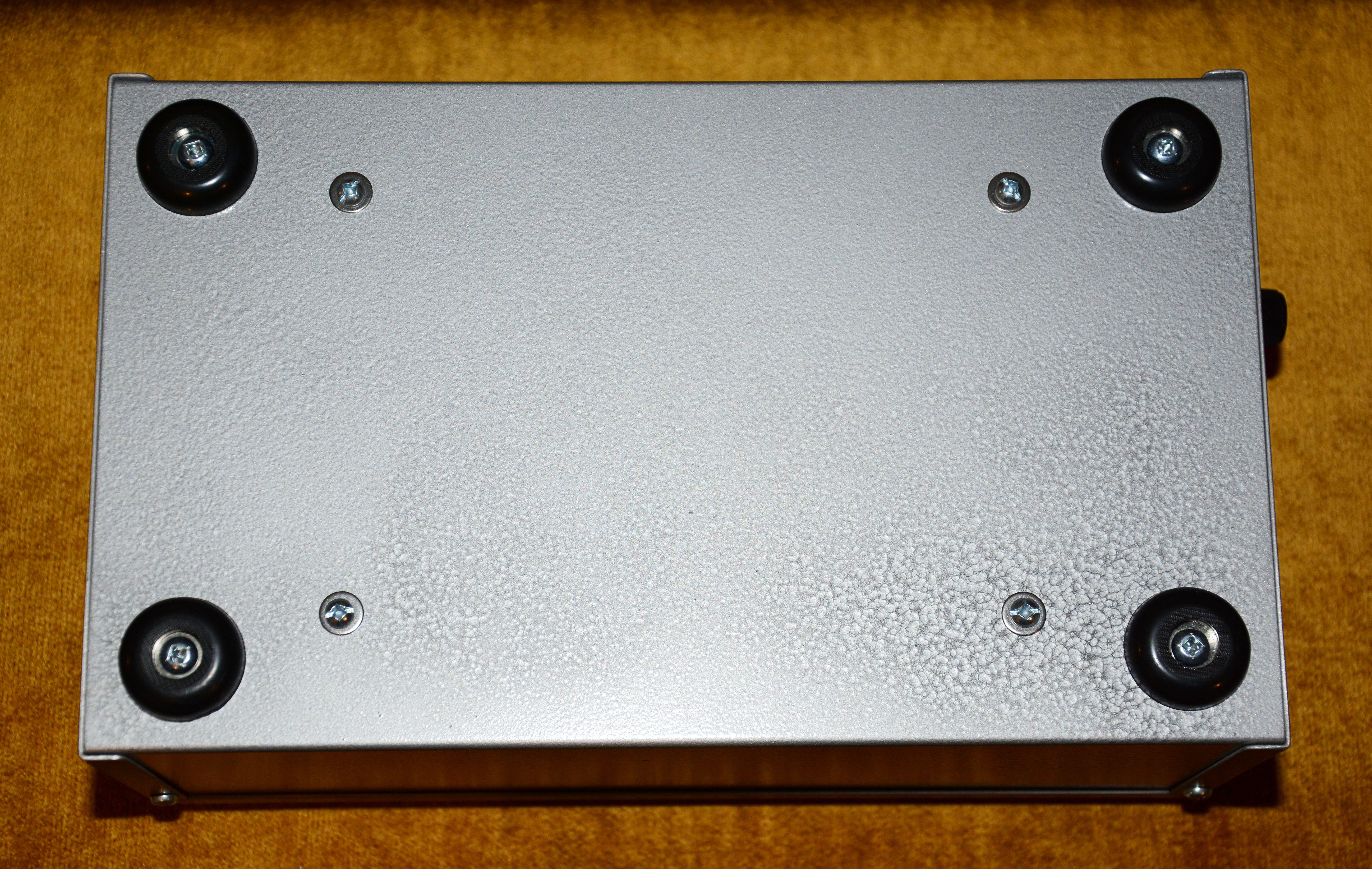
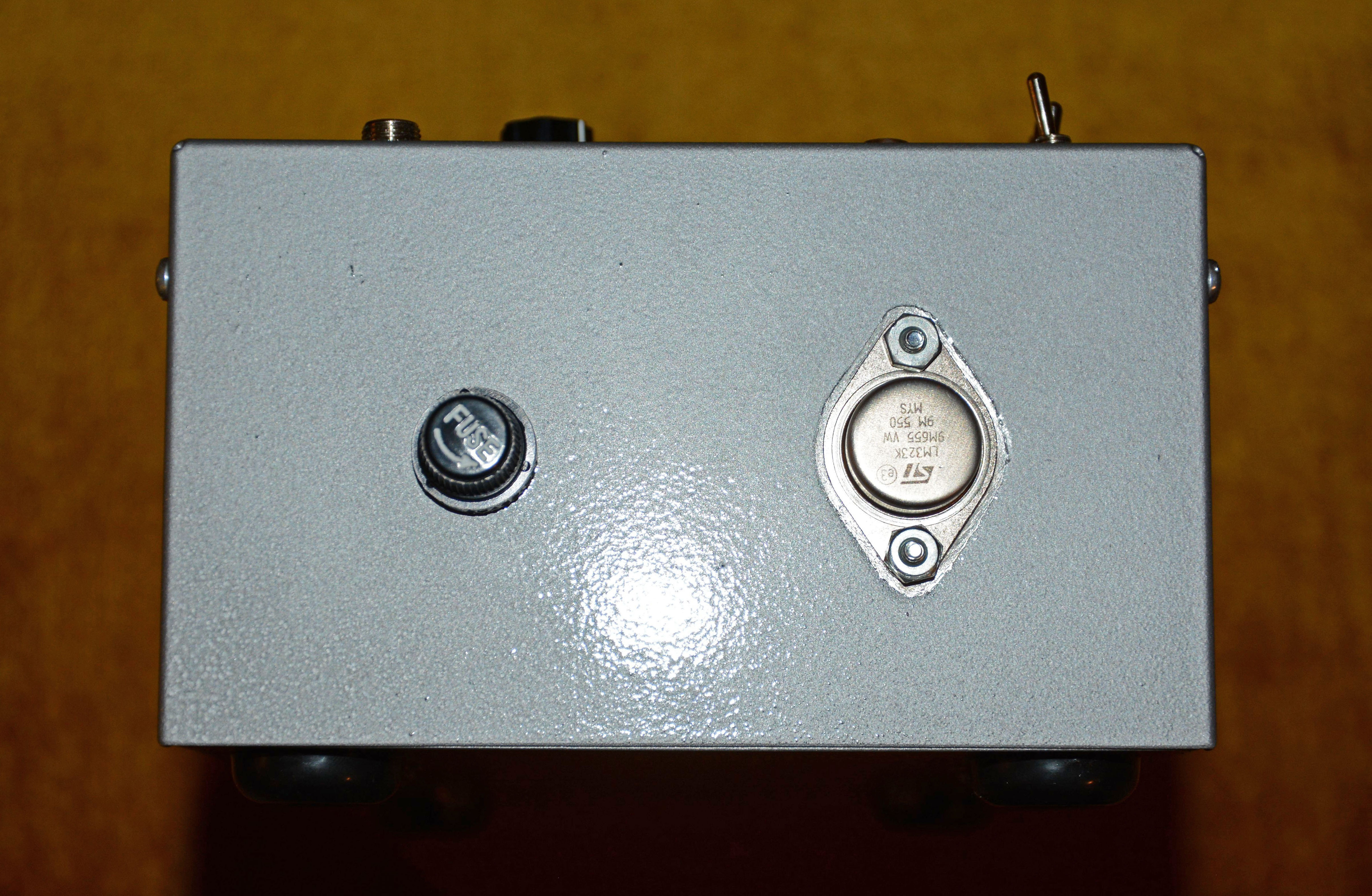
On the bottom of the enclosure, four rubber feet are attached with bolts, and the screws securing the board's posts are visible. The side has two components mounted: the fuse holder, and the LM323K 5-volt regulator. The area under the regulator was masked during painting so that the heat wouldn't be transferred through a layer of paint, and so that silicone heat transfer compound could be applied between bare metal surfaces. The enclosure itself partially acts as the regulator's heatsink, but I also put a heatsink on the inside (with heat transfer compound as well) to try to keep the enclosure from warming up too much, at least in such a small area.
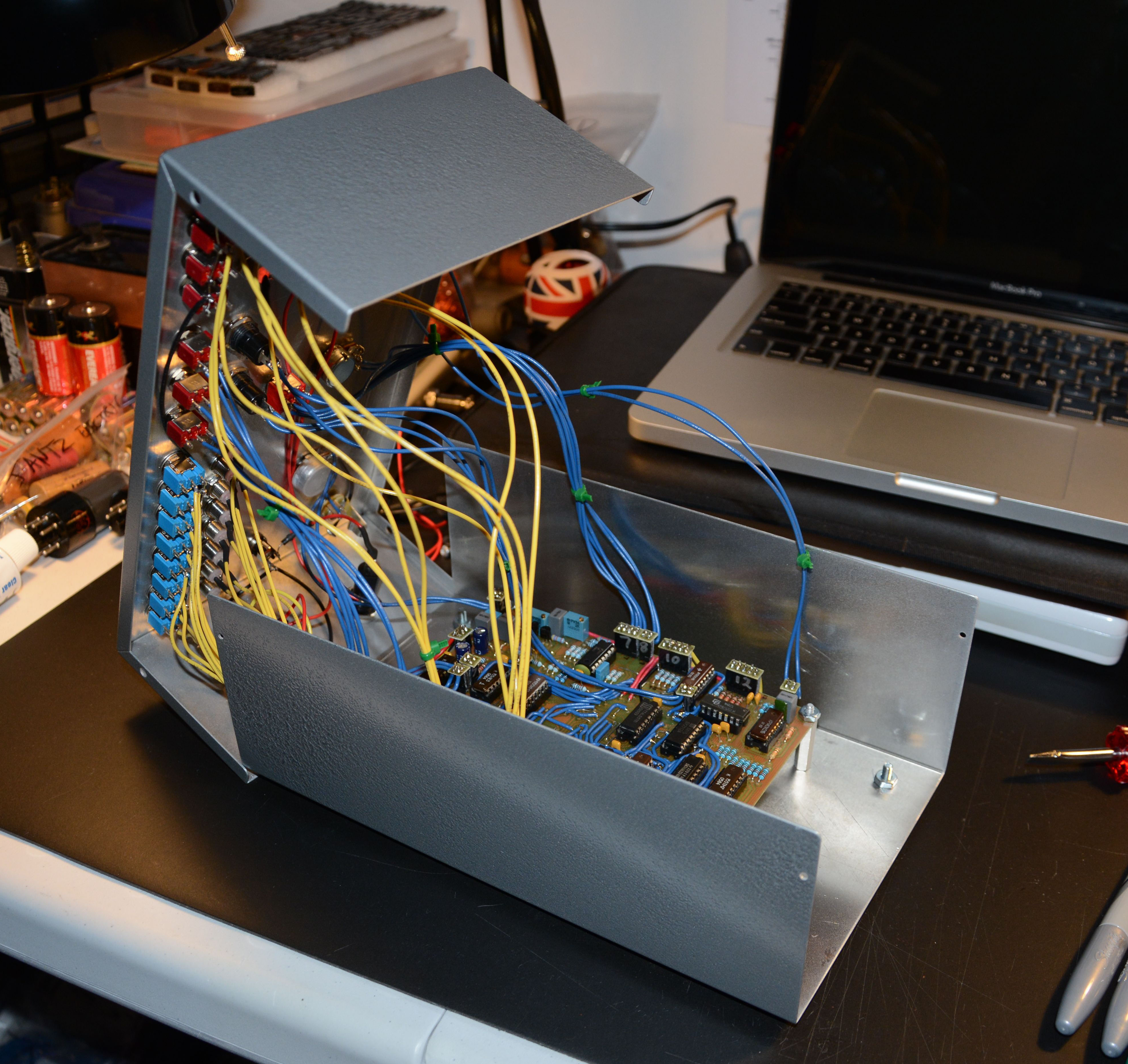
Wiring was done in a way such that the top panel can be rotated 90 degrees to the left side with all wires still attached, exposing all components for ease of service. The wires can also be easily removed from the PCB since each group of wires has its own removable connectors. These connectors are made with male and female pin headers; the male headers are on the main PCB, while the female headers are soldered to some very small PCB sections that make gripping the connectors easier, and to which the wires are also soldered. This arrangement is very inexpensive, since single-row 40-pin headers can be purchased very cheap and cut to whatever width is necessary. However, while the male headers can be split without any loss of pins, while the female headers will lose one pin every time they are split.
VideosTwo videos have been made of the BN-1: one of the prototype, and the other of the finished product. These videos include some basic demos of the sounds of the unit, in unprocessed form. They can be seen below: Downloads
|
| If you notice any errors or have additional information that you would like to add, please contact me! |